|
Silicon-based photonics technology can integrate optics and electrical devices on the same chip. A photonic link composed of a silicon photonic device such as a silicon waveguide, a modulator, an optical switch, or a detector can realize high-speed, large-capacity on-chip optical communication, and can meet the increasing demand for low power consumption, low cost, high speed, etc. of the optical communication system.
As an important device for on-chip light-electric signal conversion, the detector has been the focus of many researchers. The role of the detector in the silicon-based link is shown in Figure 1. The light wave incident through the silicon waveguide forms a light intensity signal under the action of the high frequency silicon-based modulator, and the modulated optical signal passes through a functioning silicon-based device (only the simplest modulator is shown in the schematic diagram). The detector link is received by the detector and converted into a high frequency electrical signal.
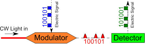
Figure 1: Modulator - Schematic diagram of detector signal transmission
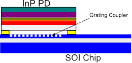
The detection of on-chip high-frequency optical signals can now be solved by a hybrid integrated III-V high-performance detector and a CMOS line integrated silicon germanium detector. The two solutions are shown in Figure 2 below:
|
|
|
|
(a) Hybrid integrated detector
|
(b) CMOS integrated silicon detector
|
Figure 2: Two detector integration schemes
In the hybrid integrated solution, the optical signal is incident on the receiving surface of the III-V detector through the Grating Coupler through the silicon waveguide to complete the detection of the optical signal. The detector is connected by reverse bonding to the top of the grating coupler. This solution enables high-sensitivity detection using the superior performance of III-V detectors.
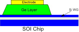
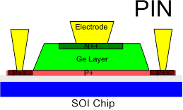
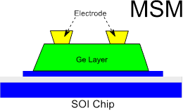
The CMOS integrated silicon germanium detector uses the absorption characteristics of germanium (Ge) materials in the 1550 nm band to detect optical signals. After passing through the silicon waveguide, the optical signal enters the germanium layer (Ge-Layer) under the action of evanescent wave coupling. In the ruthenium layer, photons are absorbed and produce electron-hole pairs. Under the action of an applied electric field, electrons and holes drift to form a current. The CMOS integrated silicon germanium detector has two typical structures, as shown in Figure 3(a)(b):
|
|
|
|
(a) Structure of a PIN type silicon germanium detector
|
(b) Structure of the MSM type detector
|
|
|
|
|
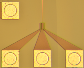
(c) Micrograph of PIN type silicon germanium detector
|
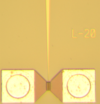
(d) Photomicrograph of the MSM detector
|
Figure 3: Two different CMOS integrated silicon detectors
The PIN-type silicon germanium detector requires a different nature of the silicon layer and the top of the germanium layer to form a vertical P-I-N junction. The electron-hole pairs generated by the photons move toward the two poles under the action of an applied electric field to form a current signal. The MSM (metal-semiconductor-metal) type detector forms a barrier structure by using a contact potential difference generated by surface contact between the metal and the tantalum material, and forms a high-low variation of the two-pole barrier under an applied bias. The electron holes generated by the photons are moved toward the two poles to output an electrical signal.
Our group has also done research on CMOS integrated silicon germanium detectors. Figure 3(c)(d) is a photomicrograph of two different types of detectors produced by our group on a CMOS process line which also showed good performance in the test.
Our group has extensive CMOS integration practice experience on silicon substrate detector implementation. There are currently two mature solutions: first, high-efficiency grating couplers with high-performance III-V detectors for high-speed, high-sensitivity detection; second, integrated silicon germanium detectors on CMOS lines Although it is slightly inferior to the III-V detector in performance, it can realize large-scale, highly integrated array detection.
|